- 您现在的位置:买卖IC网 > Sheet目录312 > AT27C256R-45PU (Atmel)IC OTP 256KBIT 45NS 28DIP
�� �
�
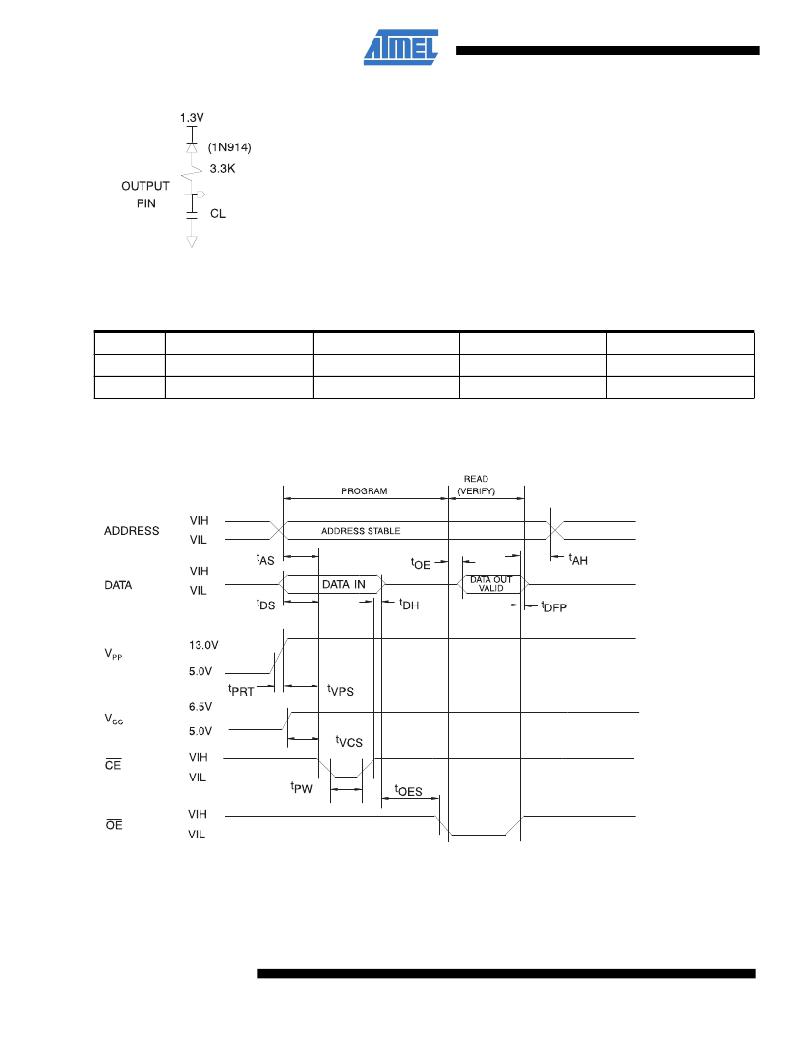
�Figure� 5-3.�
�Output� test� load�
�Note:�
�1.� C� L� =� 100pF� including� jig� capacitance,� except� for� the� -45� devices,� where� C� L� =� 30pF.�
�Table� 5-5.�
�Pin� capacitance�
�f� =� 1MHz,� T� =� 25°C� (1)�
�Symbol�
�C� IN�
�C� OUT�
�Typ�
�4�
�8�
�Max�
�6�
�12�
�Units�
�pF�
�pF�
�Conditions�
�V� IN� =� 0V�
�V� OUT� =� 0V�
�Note:�
�1.� Typical� values� for� nominal� supply� voltage.� This� parameter� is� only� sampled,� and� is� not� 100%� tested.�
�Figure� 5-4.�
�Programming� Waveforms� (1)�
�Notes:�
�1.� The� input� timing� reference� is� 0.8V� for� V� IL� and� 2.0V� for� V� IH� .�
�2.� t� OE� and� t� DFP� are� characteristics� of� the� device,� but� must� be� accommodated� by� the� programmer.�
�3.� When� programming� the� Atmel� AT27C256R,� a� 0.1μF� capacitor� is� required� across� V� PP� and� ground� to� suppress� spurious� volt-�
�age� transients.�
�6�
�Atmel� AT27C256R�
�0014O–EPROM–10/11�
�发布紧急采购,3分钟左右您将得到回复。
相关PDF资料
AT27C4096-90PU
IC OTP 4MBIT 90NS 40DIP
AT27C512R-45JU
IC OTP 512KBIT 45NS 32PLCC
AT27C516-70JI
IC OTP 512KBIT 70NS 44PLCC
AT27LV010A-70JU
IC OTP 1MBIT 70NS 32PLCC
AT27LV020A-12JU
IC OTP 2MBIT 120NS 32PLCC
AT27LV040A-90JU
IC OTP 4MBIT 90NS 32PLCC
AT27LV256A-90JU
IC OTP 256KBIT 90NS 32PLCC
AT27LV512A-90JU
IC OTP 512KBIT 90NS 32PLCC
相关代理商/技术参数
AT27C256R-45RC
功能描述:IC OTP 256KBIT 45NS 28SOIC RoHS:否 类别:集成电路 (IC) >> 存储器 系列:- 标准包装:32 系列:- 格式 - 存储器:闪存 存储器类型:FLASH 存储容量:1M (128K x 8) 速度:120ns 接口:并联 电源电压:2.7 V ~ 3.6 V 工作温度:0°C ~ 70°C 封装/外壳:32-LCC(J 形引线) 供应商设备封装:32-PLCC 包装:管件 其它名称:AT49BV00112JC
AT27C256R-45RI
功能描述:可擦除可编程ROM 256Kb (32Kx8) OTP 5V 45ns RoHS:否 制造商:Maxim Integrated 类型: 存储容量:1024 bit 组织:1 K x 1 接口类型: 工作电流:5 uA 编程电压: 工作电源电压:2.8 V to 6 V 最大工作温度:+ 85 C 安装风格:Through Hole 封装 / 箱体:TO-92
AT27C256R-45RU
功能描述:可擦除可编程ROM 256Kb (32Kx8) OTP 5V 45ns RoHS:否 制造商:Maxim Integrated 类型: 存储容量:1024 bit 组织:1 K x 1 接口类型: 工作电流:5 uA 编程电压: 工作电源电压:2.8 V to 6 V 最大工作温度:+ 85 C 安装风格:Through Hole 封装 / 箱体:TO-92
AT27C256R-45TC
功能描述:可擦除可编程ROM 256k bit RoHS:否 制造商:Maxim Integrated 类型: 存储容量:1024 bit 组织:1 K x 1 接口类型: 工作电流:5 uA 编程电压: 工作电源电压:2.8 V to 6 V 最大工作温度:+ 85 C 安装风格:Through Hole 封装 / 箱体:TO-92
AT27C256R-45TI
功能描述:可擦除可编程ROM 256Kb (32Kx8) OTP 5V 45ns RoHS:否 制造商:Maxim Integrated 类型: 存储容量:1024 bit 组织:1 K x 1 接口类型: 工作电流:5 uA 编程电压: 工作电源电压:2.8 V to 6 V 最大工作温度:+ 85 C 安装风格:Through Hole 封装 / 箱体:TO-92
AT27C256R-45TU
功能描述:可擦除可编程ROM 256Kb (32Kx8) OTP 5V 45ns RoHS:否 制造商:Maxim Integrated 类型: 存储容量:1024 bit 组织:1 K x 1 接口类型: 工作电流:5 uA 编程电压: 工作电源电压:2.8 V to 6 V 最大工作温度:+ 85 C 安装风格:Through Hole 封装 / 箱体:TO-92
AT27C256R-55
制造商:ATMEL 制造商全称:ATMEL Corporation 功能描述:256K 32K x 8 OTP CMOS EPROM
AT27C256R-55DC
制造商:未知厂家 制造商全称:未知厂家 功能描述:x8 EPROM